With the development of lithographic microfabrication and micromachining techniques, silicon carbide (SiC) has become a principal construction material in microelectromechanical systems (MEMS) [1] When the dimensions shrink to nanoscale, the ratio of surface area to volume greatly increases so that the interfacial forces become dominant [2]. As a result, the nanotribological problems involving friction, adhesion, and wear, have become an important concern in SiC-MEMS [3].
As a well-known tribological process, running-in is usually defined as the initial operation of a friction pair until certain friction force and wear rate have reached a steady state [4]. In macroscale devices, surface roughness, apparent defects, and surface waviness induced by manufacturing can affect running-in behavior [5,6]. Many new machine parts, such as cylinders and gears, often need to be conditioned through running-in before they are placed into regular service. During running-in, because the peaks of asperities on rough contact surfaces are removed by mechanical interactions and valleys are filled by wear debris, the average surface roughness of specimens would decrease to a stable state. The generation of wear debris as a three-body layer might lubricate contact interfaces [7]. As a result, both the friction force and the wear rate may decrease and then level off during macroscale running-in.
However, when tests are performed at nanoscale, counter pair normally contact with a single asperity mode due to nanoscale roughness and nanoscale contact area. In this case, the traditional running-in mechanism may not be valid during nanowear process. Nevertheless, similar to running-in processes in macroscale devices, running-in processes in nanoscale devices are often observed [8]. Therefore, it is essential to understand the running-in process in the friction pair of nanoscale devices and the variation of the friction force and wear during initial sliding cycles.
In this study, the running-in process of single crystalline silicon carbide coated with native oxide (SiC–SiOx) against a SiO2 microsphere was investigated using an atomic force microscope in ambient air. The mechanism is discussed based on an analysis of the friction-induced reduction of adhesion of the SiC–SiOx/SiO2 pair. Finally, a phenomenological model based on the results for friction and nanowear is proposed to explain the running-in process of the SiC–SiOx/SiO2 pair in ambient air.
Wafers of p-SiC(100) with a thickness of 0.5 mm were sourced from MEMC Electronic Materials, Inc., USA. The surface roughness of each silicon carbide wafer was approximately 0.07 nm over a 500 × 500 nm area. To mimic real-world MEMS surfaces, the native oxide layers on the silicon carbide surfaces were left intact. Each surface featured partial coverage of SiC–OH groups, exhibiting hydrophilic properties with a water contact angle of 39°. This substrate is referred to as “SiC–SiOx”. For comparison, a hydrophobic silicon carbide sample was prepared by immersing the original silicon carbide in a 40% aqueous hydrofluoric acid solution for 2 minutes, followed by rinsing in distilled water and methanol [4,5]. The resulting surface, denoted as “SiC–H”, displayed hydrophobic properties with a water contact angle of 83° due to the presence of SiC–H groups.
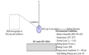
Nanowear tests were conducted on native oxide-coated silicon carbide wafers against SiO2 tips (SiC–SiOx/SiO2 pair) using an atomic force microscope (AFM, SPI3800N, Seiko, Japan) in a controlled environment chamber. As illustrated in Figure 1, the SiO2 tip with a 1 \(\mu\)m radius (Novascan Technologies, USA) moved horizontally on the silicon carbide wafer surface under a normal load Fn. The inset images show SEM micrographs of the SiO2 microsphere and its cantilever. Calibrating the normal spring constants of the SiO2 tip cantilever using a probe with a force constant of 2.957 N/m yielded values between 10.5–13.8 N/m [1]. Unless specified otherwise, the applied normal load Fn was 5 \(\mu\)N, the sliding speed was 0.8 \(\mu\)m/s, the number of sliding cycles was 2000, and the displacement amplitude D was 100 nm. The total sliding distance per cycle was 4D. All tests were performed in air with a relative humidity (RH) of 50%–60% and room temperature of 20 °C–25 °C. Friction forces were calibrated using a silicon grating with a wedge angle of 54°44’ (TGF11, MikroMasch, Germany) [14]. The adhesive behavior of the SiC–SiOx/SiO2 pair was characterized by averaging adhesion forces Fa from twenty pull-off tests. Following nanowear tests, the wear area topography was scanned using a sensitive silicon nitride tip (MLCT, Veeco, USA) with a curvature radius of 20 nm and a nominal spring constant of 0.1 N/m.
To investigate the running-in process of the SiC-SiOx/SiO2 pair, nanowear tests were conducted under various normal loads and displacement amplitudes. The friction force and wear rate were monitored during the initial 2000 sliding cycles. The results showed a significant reduction in friction force and wear rate during the initial cycles, followed by a steady state. The running-in mechanism was attributed to the reduction of adhesion-related interfacial force between the SiC-SiOx/SiO2 pair.
The wear area topography was characterized using the sensitive silicon nitride tip. The results showed a significant reduction in surface roughness and the formation of a wear-induced hydrophobic surface. The average adhesion forces Fa were obtained from twenty pull-off tests, showing a significant reduction in adhesion force after nanowear tests.
A phenomenological model was proposed to explain the running-in process of the SiC-SiOx/SiO2 pair. The model considered the reduction of adhesion-related interfacial force, surface roughness, and wear-induced hydrophobicity. The results of this study provide valuable insights into the nanotribological behavior of SiC-SiOx/SiO2 pair and can help mitigate wear failure in dynamic MEMS devices.
The friction loops and forces for the SiC-SiOx/SiO2 pair are plotted as a function of the number of sliding cycles N in Figure 2. The friction loops presented four different shapes over various numbers of sliding cycles, as shown in the inset pictures of Figure 2. During the first several cycles, the friction loop was in a parallelogram shape, which has been observed elsewhere. At the fifth cycle, the parallelogram quickly changed to the shape of an hourglass. After 50 cycles, an ellipse shape with force peaks appeared. When the number of sliding cycles increased to about 200, the friction loops finally changed to an oblique parallelogram, which was preserved throughout the remaining cycles.
Because the shape of the friction loop changed as N increased, the friction force Ft could not be calculated by simply taking the force difference between the forward and backward directions and dividing by two. Instead, the average Ft was calculated by dividing the total energy dissipated in a sliding cycle (E) by the total sliding distance per cycle (4D):
\[Ft = \frac{E}{4D}\tag{1}\]Ft = E / (4D)
In the first cycle, the friction force Ft of the SiC-SiOx/SiO2 pair was 3.9 \(\mu\)N. As the number of sliding cycles N increased, Ft exhibited a sharp decrease during the first 50 cycles, gradually decreased between 50 and 300 cycles, and then maintained a stable value in the remaining cycles up to N = 2000. Compared to Ft in the first cycle, the stable value of the friction force decreased by about 62% after the running-in process.
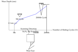
The change in shape of the friction loops shown in Figure 2 is related to the wear of the silicon carbide surface [18]. After the nanowear tests, the resulting wear scars were scanned with a sharp Si3N4 tip, as shown in Figure 3. Although the contact pressure (1.3 GPa) between the SiO2 tip and the silicon carbide surface under a normal load of 5 \(\mu\)N was far less than the yield limit of monocrystalline silicon carbide (7 GPa), material loss occurred and, after only five sliding cycles, a groove with a depth of 1.3 nm was created on the silicon carbide surface. As the number of sliding cycles increased, wear on the silicon carbide surface became more severe, and the wear depth increased to 55 nm after 2000 cycles.
To quantitatively characterize the wear behavior of the silicon carbide surface during the running-in process, the wear rate \(\gamma\) was calculated by:
\[\gamma = \frac{\Phi}{n \cdot a \cdot (F_t – F) \cdot l}\tag{2}\] \[\Phi = \gamma \cdot n \cdot a \cdot (F_t – F) \cdot l\tag{3}\] \[n = \frac{\Phi}{\gamma \cdot a \cdot (F_t – F) \cdot l}\tag{4}\] \[a = \frac{\Phi}{\gamma \cdot n \cdot (F_t – F) \cdot l}\tag{5}\] \[F_t = \frac{\Phi}{\gamma \cdot n \cdot a \cdot l} + F\tag{6}\] \[l = \frac{\Phi}{\gamma \cdot n \cdot a \cdot (F_t – F)}\tag{7}\]
where \(\phi\) is the wear volume, n is the number of sliding cycles, a is the contact area, Ft is the friction force, F is the normal load, and l is the total sliding distance (= 4D * N). As shown in Figure 3, the wear rate \(\gamma\) of the silicon carbide surface underwent a sharp drop during the initial 50 sliding cycles, then gradually decreased to a constant value over the remaining cycles.
To investigate the effects of experimental conditions on the running-in process, tests were performed at various normal loads Fn and displacement amplitudes D in humid air. Figure shows Ft-N curves of the SiC-SiOx/SiO2 pair obtained at normal loads of 0.5 \(\mu\)N, 3 \(\mu\)N, and 5 \(\mu\)N. The inset picture shows the friction coefficient \(\mu\) as a function of sliding cycles under the three loads. Here, \(\mu\) was determined by \(\mu\) = Ft/L, where L is the sum of the normal load Fn and the adhesion force Fa between tip and silicon carbide sample. As the number of sliding cycles increased, both the friction force Ft and the friction coefficient \(\mu\), at all tested loads, exhibited a sharp drop within the initial 50 cycles, then gradually decreased to stable values during the remaining cycles. Compared to the initial friction force, the stable friction force was reduced by 74%, 69%, and 62% at normal loads of 0.5 \(\mu\)N, 3 \(\mu\)N, and 5 \(\mu\)N, respectively. When the normal load was lower, the degree of friction reduction was larger.
Figure shows wear scars on the silicon carbide surface after 2000 cycles. Grooves having depths of 19 nm, 40 nm, and 55 nm were generated on the silicon carbide surface under applied normal loads of 0.5 \(\mu\)N, 3 \(\mu\)N, and 5 \(\mu\)N, respectively. However, the friction loops at 2000 cycles presented different behaviors under the three displacement amplitudes D tested. When D = 100 nm or 250 nm, the vertical section of the wear scars showed a camber shape and the friction loops formed an oblique parallelogram at 2000 cycles. But when D = 500 nm, the vertical section of the wear scars was in a U slot shape. Since the wear scar had enough space for SiO2 tip sliding, the friction force exhibited stable values within the central 400 nm and revealed peaked forces at the edges of the wear scars. These results indicate that the shape of the friction loop of SiC-SiOx/SiO2 pair was strongly dependent on the topography of wear scars on the silicon carbide surface.
Figure exhibits Ft-N curves of the SiC-SiOx/SiO2 pair at displacement amplitudes D of 100, 250, and 500 nm. Similar to that at D = 100 nm and Fn = 5 \(\mu\)N, the friction force decreased by about 62% during running-in processes at D = 250 and 500 nm. After 2000 cycles, grooves with depths of about 55 nm were formed regardless of the displacement amplitude. Clearly, the influence of D (> 100 nm) on the friction behavior of the SiC-SiOx/SiO2 pair and on wear of the silicon carbide surface was negligible.
To investigate the effect of humidity on the running-in process, tests were performed in dry air (RH < 5%) and humid air (RH = 50-60%). Ft-N curves of the SiC-SiOx/SiO2 pair obtained in dry air and humid air. The friction force in dry air was higher than that in humid air during the initial 50 cycles. However, the friction force in both environments converged to a similar stable value after 200 cycles. The wear rate \(\gamma\) in dry air was slightly higher than that in humid air. The wear scars on the silicon carbide surface after 2000 cycles in both environments were similar, with depths of about 55 nm.
The running-in process of the SiC-SiOx/SiO2 pair at the nanoscale is characterized by a sharp drop in friction force and wear rate during the initial sliding cycles. This behavior is attributed to the removal of the native oxide layer on the silicon surface and the subsequent hydrophobization of the contact area. The experimental results show that the friction force decreases significantly during the initial 50 cycles, followed by a stable friction force [8,9]. This suggests that the running-in process is completed within the first 50 cycles, and the frictional behavior becomes stable thereafter.
The effect of normal load on the running-in process was investigated, and the results show that the friction force decreases with increasing normal load. This is attributed to the increased contact pressure, which enhances the removal of the native oxide layer and the hydrophobization of the contact area. The displacement amplitude was also varied, and the results show that the friction force decreases with increasing displacement amplitude. This is attributed to the increased sliding distance, which enhances the removal of the native oxide layer and the hydrophobization of the contact area [10].
The effect of humidity on the running-in process was investigated, and the results show that the friction force is higher in dry air than in humid air. This is attributed to the increased capillary force in humid air, which enhances the removal of the native oxide layer and the hydrophobization of the contact area. The proposed mechanism for the running-in process involves the formation of a water bridge between the SiC-SiOx substrate and the SiO2 tip surface, followed by the removal of the native oxide layer via water-induced corrosion. The exposed silicon surface becomes more hydrophobic, reducing the friction force and wear rate [11].
The results of this study provide insight into the tribological behavior of nanoscale devices and highlight the importance of considering tribochemical reactions in the design and operation of such devices. The running-in process is critical in determining the frictional behavior of nanoscale devices, and understanding this process is essential for optimizing their performance [12]. The frictional behavior of the SiC-SiOx/SiO2 pair is dependent on the experimental conditions, including normal load, displacement amplitude, and humidity. This suggests that the frictional behavior of nanoscale devices can be tailored by controlling the experimental conditions.
The hydrophobization of the contact area is a critical factor in determining the frictional behavior of the SiC-SiOx/SiO2 pair. The results show that the friction force decreases significantly when the contact area becomes hydrophobic, suggesting that hydrophobization is essential for reducing friction in nanoscale devices. The results of this study have implications for the design and operation of nanoscale devices, such as MEMS/NEMS and BioMEMS/BioNEMS. Understanding the running-in process and the factors that influence it is essential for optimizing the performance of these devices and ensuring their reliable operation.
The removal of the native oxide layer is a critical step in the running-in process, as it exposes the silicon surface and allows for hydrophobization to occur. This process is enhanced by the water-induced corrosion mechanism, which is promoted by the presence of water molecules in the contact area. The hydrophobization of the contact area is a result of the dehydroxylation reactions that occur during the sliding process. These reactions lead to the formation of siloxane bonds, which are more hydrophobic than the silanol bonds present on the native oxide layer [4,9].
The frictional behavior of the SiC-SiOx/SiO2 pair is also influenced by the surface roughness of the silicon substrate. A smoother surface leads to a higher friction force, as there is a greater contact area between the substrate and the SiO2 tip. The wear rate of the silicon substrate is also influenced by the running-in process. The wear rate decreases significantly after the initial 50 cycles, suggesting that the running-in process leads to a more stable wear behavior.
The results of this study have implications for the development of nanoscale devices that operate in humid environments. The presence of water molecules can lead to increased friction and wear, but the running-in process can help to mitigate these effects. The running-in process is not unique to the SiC-SiOx/SiO2 pair, as similar behavior has been observed in other nanoscale systems. This suggests that the running-in process is a general phenomenon that can occur in a variety of nanoscale systems [4,10].
The frictional behavior of nanoscale devices is often dominated by adhesion forces, which can lead to high friction coefficients. The running-in process can help to reduce these adhesion forces, leading to a decrease in the friction coefficient. The wear behavior of nanoscale devices is also influenced by the running-in process. The wear rate can decrease significantly after the initial running-in period, leading to a more stable wear behavior [].
The results of this study demonstrate the importance of considering tribochemical reactions in the design and operation of nanoscale devices. These reactions can lead to significant changes in the frictional behavior and wear rate of nanoscale systems. The running-in process is a critical factor in determining the reliability and performance of nanoscale devices. Understanding this process is essential for optimizing the design and operation of these devices, and for ensuring their reliable operation in a variety of environments.
the running-in process of the SiC-SiOx/SiO2 pair at the nanoscale is a complex phenomenon that involves the removal of the native oxide layer, hydrophobization of the contact area, and changes in the surface roughness of the silicon substrate. The experimental results show that the friction force decreases significantly during the initial 50 cycles, followed by a stable friction force. The running-in process is influenced by the normal load, displacement amplitude, and humidity, and is critical in determining the frictional behavior and wear rate of nanoscale devices. The proposed mechanism for the running-in process involves the formation of a water bridge between the SiC-SiOx substrate and the SiO2 tip surface, followed by the removal of the native oxide layer via water-induced corrosion. The exposed silicon surface becomes more hydrophobic, reducing the friction force and wear rate. The results of this study provide insight into the tribological behavior of nanoscale devices and highlight the importance of considering tribochemical reactions in the design and operation of such devices.
The findings of this study have significant implications for the development of nanoscale devices, such as MEMS/NEMS and BioMEMS/BioNEMS. Understanding the running-in process and the factors that influence it is essential for optimizing the performance of these devices and ensuring their reliable operation. The results of this study demonstrate the importance of considering the tribological behavior of nanoscale devices in the design and operation of these systems. Furthermore, the results of this study suggest that the running-in process is not unique to the SiC-SiOx/SiO2 pair, but is a general phenomenon that can occur in a variety of nanoscale systems. This highlights the importance of considering the running-in process in the design and operation of nanoscale devices, regardless of the materials used.
In summary, the running-in process is a critical factor in determining the frictional behavior and wear rate of nanoscale devices. Understanding this process is essential for optimizing the design and operation of these devices, and for ensuring their reliable operation in a variety of environments. The results of this study provide valuable insights into the tribological behavior of nanoscale devices and highlight the importance of considering tribochemical reactions in the design and operation of these systems.