To achieve higher recording density, the flying height of head sliders over magnetic disks in hard disk drives is progressively decreasing annually. This necessitates thinner, more wear-resistant coatings to prevent data loss caused by sliding contact [1]. While DLC has been used, the search for superior overcoat materials continues. Carbon nitride (CNx) has emerged as a promising candidate due to its superior tribological properties compared to DLC. Further research highlighted the intriguing load dependence of CNx specific wear amount, contrasting with the load-independent behavior of carbon films. This disparity is attributed to differences in material properties and/or nanoscale wear mechanisms. To investigate these mechanisms, scratch tests and atomic force microscopy (AFM) are valuable tools for examining wear properties at the nanoscale. Previous AFM-based scratch tests have successfully characterized wear in materials such as amorphous carbon and nitrogen-implanted silicon. This study employs an AFM tribotester to explore the influence of coating conditions, contact load, tip pin radius, and contact pressure on the nanoscale wear properties of CNx sliding against a diamond pin [2].
Understanding the wear mechanisms of these thin coatings at the nanoscale is crucial for developing more resilient and durable hard disk drives. By subjecting CNx coatings to controlled wear conditions and meticulously analyzing the resulting wear scars, this research aims to elucidate the factors influencing the wear behavior of this promising material [3]. The insights gained from this study are expected to contribute to the optimization of CNx coatings for enhanced tribological performance in high-density storage devices.
The findings of this research could have broader implications for the development of other protective coatings in various applications where wear resistance is paramount. By unraveling the wear mechanisms of CNx, researchers can potentially identify strategies to improve the durability of coatings in fields such as aerospace, automotive, and biomedical engineering. This study serves as a foundation for future investigations into the tribological behavior of advanced materials and coatings.
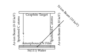
Amorphous carbon nitride (CN) films were deposited on Si(111) wafers using the ion beam-assisted deposition (IBAD) technique. This method involves the simultaneous sputtering of carbon by an argon-ion beam and the irradiation of nitrogen ions. The energy of the sputtered ions ranged from 0 to 10 keV, with ion current densities varying from 0 to 40 mA/cm². The optimal coating conditions were identified as 0.5 keV ion energy and 40 mA/cm² current density, resulting in a deposition rate of approximately 1.4 nm/min. The nitrogen ion energy was set to 10 keV, with an incident angle of 45° relative to the substrate.
The deposition of amorphous carbon nitride (CN) films was accomplished using the Ion Beam-Assisted Deposition (IBAD) technique, a method that combines physical vapor deposition (PVD) with ion irradiation to enhance film adhesion and modify its properties.
Step 1: Substrate Preparation
The substrates used for coating were Si(111) wafers, chosen for their crystalline orientation, which provides a suitable foundation for film growth. Prior to deposition, the substrates underwent rigorous cleaning, including ultrasonic cleaning in acetone and isopropanol, followed by drying in a nitrogen stream, ensuring a contaminant-free surface.
Step 2: Carbon Sputtering
The process commenced with the sputtering of carbon atoms from a graphite target. An argon-ion beam, generated using a Kaufman-type ion source, was directed at the target. The sputtering energy ranged between 0 to 10 keV, finely tuned to control the ejection of carbon atoms. The ion current density was varied from 0 to 40 mA/cm², allowing for precise control over the deposition rate. Under optimal conditions, a carbon ion energy of 0.5 keV and a current density of 40 mA/cm² were maintained, resulting in a deposition rate of approximately 1.4 nm/min.
Step 3: Nitrogen Ion Irradiation
Simultaneously with carbon sputtering, nitrogen ions were irradiated onto the growing film. The nitrogen ions, with an energy level set at 10 keV, were directed at the substrate at a 45° angle. This angle was chosen to maximize the incorporation of nitrogen into the carbon matrix, facilitating the formation of CN bonds and thus modifying the mechanical properties of the film.
Step 4: Coating Formation
The interaction between the sputtered carbon atoms and the nitrogen ions resulted in the formation of a dense amorphous CN film. The nitrogen atoms were embedded into the carbon lattice, forming a hybrid structure with both sp2 and sp3 bonds. This hybrid bonding structure is crucial for achieving the desired wear-resistant properties.
Step 5: Post-Deposition Treatment
After deposition, the CN-coated wafers were subjected to a post-deposition annealing process at 200°C for 2 hours in a vacuum chamber. This step was essential for relieving internal stresses and enhancing the film’s adhesion to the substrate.
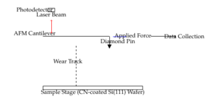
Wear tests were conducted using a commercial AFM, with a diamond pin attached to a cantilever. The cantilever’s deflection was measured using a laser deflection technique. Different diamond pins with radii of 90 nm, 150 nm, and 270 nm were used in scratching tests to vary the contact pressure. The wear depth was monitored during the tests, and the specific wear amounts were calculated based on the wear depth and the scratched area.
The micro-wear tests were conducted using a high-precision Atomic Force Microscope (AFM) equipped with a custom attachment for micro-wear testing. The AFM setup included a diamond pin, which was affixed to the end of a cantilever. This setup allowed for precise control over the contact load and ensured accurate measurement of wear depth during the sliding tests.
The cantilever, an essential component of the AFM, was designed to be both stiff and sensitive. It was equipped with a diamond pin, which acted as the indenter and wear probe. The diamond pin had a tip radius of 90 nm, 150 nm, or 270 nm, depending on the specific test conditions. This variation in pin radius allowed for the investigation of different contact pressures during the wear tests.
The deflection of the cantilever was monitored using a laser beam. A laser was directed at the back of the cantilever, and its reflection was captured by a position-sensitive photodetector. This setup allowed for real-time monitoring of the cantilever’s deflection, which correlated directly with the force applied during the wear tests.
The CN-coated Si(111) wafers were securely mounted on the AFM sample stage. The mounting process ensured that the samples were flat and stable, preventing any movement that could affect the accuracy of the wear measurements. The sample stage was also equipped with a heating system, allowing for temperature control during testing, if necessary.
During the wear tests, the diamond pin was brought into contact with the CN-coated wafer. The AFM operated in contact mode, where the pin was dragged across the surface under a controlled load. The load was varied from low to high to examine its effect on wear behavior. The scanning direction was typically linear, and the test duration was set to ensure measurable wear without causing complete coating failure.
The wear depth was measured by analyzing the topographical changes in the CN coating post-test. The AFM’s high-resolution imaging capabilities allowed for precise measurement of the wear track’s depth and width. The specific wear amount was calculated by dividing the wear volume by the product of the load and sliding distance.
The collected data was analyzed to determine the relationship between wear depth, contact load, and pin radius. Statistical methods were employed to ensure that the results were reproducible and to identify any significant trends or anomalies in the data.
Chemical analysis using secondary ion mass spectrometry (SIMS) revealed that the nitrogen content in CN coatings was relatively high and uniform throughout the thickness of the coating. Raman spectroscopy indicated that the structure of CN is a mixture of sp2 and sp3 bonding.
Surface roughness of the CN films was measured using Atomic Force Microscopy (AFM) in tapping mode. The AFM was equipped with a sharp silicon tip, oscillating close to its resonance frequency. This technique allowed for non-destructive profiling of the surface, capturing height variations at the nanometer scale. The roughness was quantified by calculating the root-mean-square (RMS) value of the surface heights over the scanned area [4].
To analyze the chemical composition of the CN films, X-ray Photoelectron Spectroscopy (XPS) was employed. The XPS system was equipped with an Al K\(\alpha\) X-ray source, providing photons at 1486.6 eV. The analysis was performed under ultra-high vacuum conditions to prevent contamination. High-resolution spectra were acquired for the carbon (C 1s) and nitrogen (N 1s) regions to determine the bonding states. The spectra were deconvoluted to identify specific bonds, such as C-C, C=N, and \(C\equiv N\).
Raman spectroscopy was used to characterize the bonding structure within the CN films. The Raman system was equipped with a 532 nm laser, which provided a non-destructive means of probing the vibrational modes of the film. The Raman spectra were collected over a range of 1000 to 3000 \(cm^{-1}\). The D and G peaks were analyzed to understand the sp² and sp³ hybridization states in the carbon network [5]. Additionally, the presence of a shoulder near the G peak indicated the incorporation of nitrogen into the carbon matrix.
Surface energy was evaluated using contact angle measurements. A goniometer was employed to measure the contact angles of water and diiodomethane droplets on the CN film surface. These angles were used to calculate the surface energy components (polar and dispersive) based on the Owens-Wendt model. The results provided insight into the film’s wettability and potential adhesive properties.
Transmission Electron Microscopy (TEM) was utilized for high-resolution imaging of the CN film’s microstructure. Cross-sectional samples were prepared using a focused ion beam (FIB) system. The TEM analysis revealed the thickness of the film and the presence of any crystalline phases or defects within the amorphous structure.
The wear depth of CN coatings increased proportionally with the number of sliding cycles, with specific wear amounts varying significantly depending on the coating conditions. A notable increase in wear depth was observed when the contact load exceeded a critical value, particularly with smaller pin radii. The specific wear amount of CN coatings increased sharply with maximum contact pressure, indicating a transition from mild wear to delamination at around 13 GPa [6]. Below 9 GPa, the specific wear amount of CN coatings was lower than that of DLC, highlighting the superior wear resistance of CN coatings under low-pressure conditions.
The wear resistance of the CN films was evaluated using a micro-wear tester integrated with an Atomic Force Microscope (AFM). A diamond tip, with a controlled normal load, was used to slide across the surface of the CN-coated Si(111) wafers. The tests were performed under various loads and sliding distances to assess the durability of the films. The wear tracks were scanned with AFM post-test to measure the wear depth and width [7].
The friction coefficient was measured simultaneously with the wear tests. As the diamond tip slid across the surface, lateral forces were recorded using the AFM’s lateral force microscopy (LFM) mode. The friction coefficient was calculated by dividing the lateral force by the normal load. This analysis provided insights into the tribological performance of the CN films under different loading conditions.
Wear volume was calculated by integrating the wear track profile obtained from AFM scans. The wear volume (V) was determined using the formula:
\[V = Area of wear track \times Sliding distance\]
This parameter was crucial in comparing the wear resistance of CN films with varying thicknesses and compositions.
Post-wear, the surface damage was characterized using Scanning Electron Microscopy (SEM) and Energy-Dispersive X-ray Spectroscopy (EDX). SEM images were captured to observe any surface cracks, delamination, or debris formation within the wear tracks. EDX was used to analyze the elemental composition within the wear tracks to identify any material transfer from the diamond tip or substrate [8].
The wear mechanisms were analyzed based on the AFM, SEM, and EDX data. Possible mechanisms included abrasive wear, adhesive wear, and fatigue wear. The wear behavior was correlated with the film’s microstructure, as revealed by the TEM analysis, and the chemical bonding information from XPS.
Eleven different carbon nitride coatings were tested under varying conditions using an AFM-based micro-wear tester. The results showed that the specific wear amount of CN coatings could vary significantly based on coating conditions, contact load, and pin radius. The best-performing CN coating was obtained under specific conditions of nitrogen ion energy and current density. The study also highlighted the importance of contact pressure in determining the wear behavior of CN coatings, with a transition to high wear observed at around 13 GPa.