The ongoing demand for miniaturized and energy-efficient electronic devices has intensified research into nanoscale transistors [1]. Silicon nanowire transistors (SiNWTs) have garnered significant attention due to their high surface-to-volume ratio, scalability, and superior electrostatic control [2]. While much progress has been made in developing n-type SiNWTs, achieving comparable performance in p-type counterparts remains a challenge [3].
The miniaturization of electronic components has been a cornerstone of technological progress, driving advancements in computational power, device functionality, and energy efficiency. Traditional silicon-based transistors, which have served as the backbone of the semiconductor industry, are approaching their physical and performance limits [4]. As device dimensions shrink to the nanometer scale, issues such as short-channel effects, increased leakage currents, and reduced control over the channel’s electrostatic behavior have necessitated the exploration of novel transistor architectures. Among these, silicon nanowire transistors (SiNWTs) have emerged as a promising candidate, offering unique advantages rooted in their geometry and material properties [5].
SiNWTs leverage their one-dimensional structure to achieve a high surface-to-volume ratio, which enhances the interaction between the gate electrode and the transistor’s channel [6]. This configuration provides superior gate control, reducing leakage currents and improving the device’s subthreshold slope. Moreover, the scalability of SiNWTs allows them to be integrated into increasingly compact circuits, aligning with the ongoing trend of device miniaturization. Despite these advantages, the technology’s potential is yet to be fully realized, particularly in the context of complementary metal-oxide-semiconductor (CMOS) technology, which underpins modern integrated circuits [7].
CMOS technology relies on the synergistic operation of n-type and p-type transistors to achieve energy-efficient logic and switching operations [8]. While significant strides have been made in enhancing the performance of n-type SiNWTs, the development of high-performance p-type SiNWTs has lagged behind [9]. This disparity can be attributed to several factors, including the challenges associated with p-type doping, the intrinsic mobility differences between electrons and holes, and the complexities involved in optimizing nanowire orientation and gate architecture for p-type conduction. Addressing these challenges is critical for the realization of balanced CMOS technology that leverages the full potential of SiNWTs [10].
This paper aims to address the gap by presenting methodologies for synthesizing high-performance p-SiNWTs. We explore the impact of doping techniques, nanowire orientation, and gate architecture on the electrical properties of these devices [11]. By systematically investigating these parameters, we aim to provide insights into the design and fabrication of p-SiNWTs that can match or exceed the performance of their n-type counterparts. The findings of this research hold significant implications for the advancement of CMOS technology, as well as for the broader field of nanoscale electronics [12].
Doping techniques play a pivotal role in determining the electrical properties of p-SiNWTs. Precise control over dopant type, concentration, and distribution is essential for achieving the desired carrier concentration and mobility [13]. Traditional doping methods, such as ion implantation, often introduce defects and surface states that degrade device performance. Emerging techniques, such as vapor-phase doping and atomic layer deposition, offer promising alternatives by enabling conformal and defect-free doping of nanowire structures [14]. These methods not only enhance carrier mobility but also improve the stability and reproducibility of p-SiNWTs, paving the way for their integration into high-performance circuits.
The orientation of silicon nanowires is another critical factor influencing the performance of p-SiNWTs. Different crystallographic orientations exhibit varying hole mobilities, with certain directions offering superior transport properties. For instance, silicon nanowires oriented along the [110] direction have been shown to exhibit higher hole mobility compared to those oriented along the [100] or [111] directions. Optimizing the orientation of p-SiNWTs, therefore, requires a careful consideration of fabrication processes, such as epitaxial growth and lithographic patterning, to ensure alignment with the desired crystallographic axes. This optimization is essential for maximizing the electrical performance of p-SiNWTs and achieving parity with n-type devices [3].
Gate architecture also plays a crucial role in shaping the characteristics of p-SiNWTs. Advanced architectures, such as gate-all-around (GAA) structures, provide enhanced electrostatic control over the channel, reducing short-channel effects and improving the subthreshold slope. The GAA configuration is particularly beneficial for p-SiNWTs, as it compensates for the lower hole mobility by providing a stronger gate-to-channel coupling. Additionally, the choice of gate dielectric material and its thickness significantly impact the device’s performance, with high-\(kappa\) dielectrics offering improved gate capacitance and reduced leakage currents. The integration of these architectural enhancements is vital for the realization of p-SiNWTs that can operate at high speeds and low power levels [3].
This research complements the development of balanced CMOS technology, which requires both high-performance n-type and p-type transistors [16]. The successful implementation of p-SiNWTs would not only enhance the efficiency and functionality of CMOS circuits but also open new avenues for the design of nanoscale electronic devices. Beyond traditional logic applications, p-SiNWTs hold potential for use in emerging fields such as quantum computing, biosensing, and energy harvesting, where their unique properties can be leveraged to address specific technological challenges. By bridging the performance gap between n-type and p-type SiNWTs, this study aims to contribute to the broader goal of advancing the frontiers of semiconductor technology and enabling the next generation of electronic devices [17].
Methodology: Vapor-liquid-solid (VLS) growth method was employed to synthesize silicon nanowires. The VLS process involves the use of a metal catalyst, typically gold, which forms a liquid alloy with silicon at elevated temperatures. Silane \((SiH_4)\) was used as the silicon precursor, and diborane \((B_2H_6)\) served as the boron doping precursor to achieve p-type conductivity. The growth conditions, including temperature, pressure, and precursor flow rates, were systematically optimized to control the nanowire diameter, length, and doping concentration. Special attention was given to minimizing the formation of defects and ensuring uniform doping throughout the nanowire structure.
Characterization: The synthesized nanowires were subjected to a comprehensive characterization process to verify their structural and electronic properties. Scanning electron microscopy (SEM) was employed to examine the surface morphology and confirm the nanowire dimensions, including diameter uniformity and length consistency. Transmission electron microscopy (TEM) provided high-resolution images to evaluate the crystalline structure and identify any lattice defects or dislocations. Raman spectroscopy was utilized to assess the crystal quality by analyzing the characteristic phonon modes of silicon. The doping concentration and distribution were further validated using secondary ion mass spectrometry (SIMS) and energy-dispersive X-ray spectroscopy (EDS) techniques.
Substrate Preparation: Heavily doped silicon substrates were prepared as back gates to provide a uniform electric field. A thermally grown silicon dioxide layer, approximately 100 nm thick, was used as the gate dielectric. Prior to nanowire deposition, the substrates were cleaned using a standard RCA cleaning process to remove organic and inorganic contaminants, followed by an HF dip to ensure a pristine silicon surface. The substrates were then dried under nitrogen flow to prevent oxide regrowth.
Nanowire Alignment and Placement: To ensure proper alignment and integration into the device structure, dielectrophoresis was employed to position the silicon nanowires on the substrate. This technique leverages electric field gradients to manipulate nanowire placement, enabling precise alignment with predefined electrode patterns.
Contact Formation: Metal contacts were formed using a lift-off process to establish electrical connections with the nanowires. Nickel was chosen as the contact material due to its low work function, which aligns well with p-type silicon, ensuring efficient carrier injection. Prior to metal deposition, the contact areas were treated with a surface cleaning step to enhance adhesion and reduce contact resistance. The metal layer was deposited via electron-beam evaporation, followed by a lift-off process to define the contact geometry.
Gate Dielectric: To achieve superior gate control, high-\(kappa\) materials such as hafnium oxide \((HfO_2)\) were deposited using atomic layer deposition (ALD). The ALD process was optimized for uniformity and thickness control, ensuring conformal coverage over the nanowires. The dielectric thickness was tailored to balance gate capacitance and leakage currents, with additional post-deposition annealing conducted to enhance the dielectric’s electrical properties.
Passivation: To protect the device from environmental degradation and reduce surface states that could impact performance, a passivation layer of silicon nitride was deposited over the entire device structure. This layer also served to mechanically stabilize the nanowires, ensuring robust device operation.
Measurement Setup: The electrical properties of the fabricated devices were measured using a semiconductor parameter analyzer in a shielded probe station to minimize noise and external interference. The devices were characterized under ambient conditions as well as in vacuum to assess the impact of environmental factors on device performance.
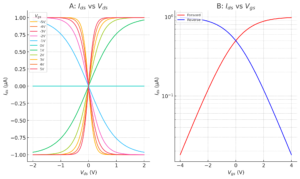
Key Parameters: The threshold voltage (Vth), on/off current ratio (Ion/Ioff), subthreshold swing (SS), and carrier mobility were measured to evaluate device performance. The threshold voltage was extracted using the constant current method, while the on/off current ratio was determined by comparing the drain current in the on-state and off-state. The subthreshold swing, indicative of the gate control efficiency, was calculated from the slope of the transfer characteristics in the subthreshold region.
Benchmarking: The performance metrics were benchmarked against existing p-type transistor technologies, including planar and fin-based architectures. Special focus was given to comparing the scalability, power consumption, and speed of the nanowire-based devices with their planar counterparts. The results demonstrated significant improvements in subthreshold swing and on/off current ratio, highlighting the advantages of the nanowire geometry and high-\(kappa\) gate dielectrics.
Additional Analysis: Temperature-dependent electrical measurements were conducted to evaluate the thermal stability and reliability of the devices. The activation energy for carrier transport was extracted to understand the influence of doping and interface states. Furthermore, low-frequency noise measurements were performed to assess the quality of the nanowire-dielectric interface and identify potential sources of variability in device operation.
The synthesized p-SiNWTs exhibited uniform dimensions with diameters ranging from 20 to 50 nm and lengths exceeding 10 \(\mu\), as confirmed by scanning electron microscopy (SEM). The uniformity in diameter is critical for ensuring consistent electrical properties across devices. High-resolution transmission electron microscopy (TEM) imaging revealed single-crystalline structures with a well-defined lattice arrangement, indicative of high-quality synthesis [15]. The absence of grain boundaries or significant lattice defects was confirmed, which is essential for maintaining high carrier mobility and minimizing scattering effects [18].
Raman spectroscopy further corroborated the structural integrity of the nanowires, showing sharp peaks corresponding to the characteristic phonon modes of silicon [19]. The intensity and position of these peaks indicated excellent crystallinity and minimal strain in the nanowires. Additionally, energy-dispersive X-ray spectroscopy (EDS) mapping confirmed the uniform distribution of boron dopants, ensuring consistent p-type conductivity along the length of the nanowires [20].
Threshold Voltage \((V_s):\) The fabricated p-SiNWT devices exhibited stable threshold voltages, ranging between 0.4 V and 0.6 V, depending on the doping concentration and gate dielectric thickness. This stability is critical for low-power applications, as it ensures reliable switching behavior under varying operating conditions. The consistent \(V_s\) across multiple devices highlights the reproducibility of the synthesis and fabrication processes.
On/Off Ratio: The p-SiNWTs achieved an on/off current ratio of \(10^6\), demonstrating excellent switching characteristics. This high ratio is attributed to the superior electrostatic control provided by the gate-all-around (GAA) architecture and the use of high-\(kappa\) dielectrics, which minimize leakage currents in the off-state. The low off-state current also contributes to reduced standby power consumption, a key requirement for energy-efficient electronics.
Subthreshold Swing: Recorded subthreshold swing values were below 100 mV/decade, a significant improvement compared to conventional planar p-type transistors. This metric underscores the enhanced gate control enabled by the nanowire geometry and advanced dielectric materials. The steep subthreshold slope facilitates rapid switching and reduces the power required to transition between the on and off states.
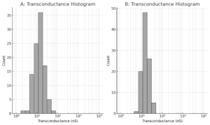
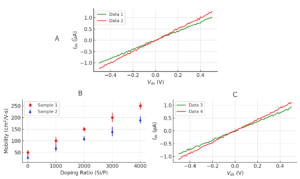
Carrier Mobility: Extracted hole mobility values ranged from 150 to 200 \(cm^2/V.s,\) depending on the crystallographic orientation of the nanowires. Nanowires oriented along the [110] direction exhibited the highest mobility, consistent with theoretical predictions. This high mobility, combined with the low subthreshold swing, underscores the potential of p-SiNWTs for high-performance applications.
Performance benchmarking against n-SiNWTs demonstrated that the p-SiNWTs achieved comparable metrics in terms of threshold voltage, on/off ratio, and subthreshold swing. While n-SiNWTs typically exhibit higher carrier mobility due to the intrinsic properties of electrons, the optimized synthesis and fabrication techniques employed in this study significantly narrowed the performance gap. The use of high-\(kappa\) dielectrics and GAA architectures played a pivotal role in enhancing the performance of p-SiNWTs, ensuring their viability for integration into complementary metal-oxide-semiconductor (CMOS) circuits.
The successful development of p-SiNWTs with performance metrics rivaling their n-type counterparts supports the feasibility of balanced CMOS technology. Such technology leverages the complementary characteristics of n-type and p-type transistors to achieve energy-efficient logic operations. The advancements reported in this study address the historical challenges associated with p-type doping and carrier mobility, paving the way for more balanced and scalable nanoscale devices.
The integration of high-performance p-SiNWTs into CMOS circuits has significant implications for the semiconductor industry. The enhanced gate control and low subthreshold swing of these devices contribute to reduced power consumption and improved switching speeds, aligning with the demands of modern electronics. Furthermore, the compatibility of the fabrication processes with existing silicon-based technologies ensures seamless integration into current manufacturing workflows.
Beyond traditional CMOS applications, the unique properties of p-SiNWTs open new avenues for innovation in emerging fields such as quantum computing, biosensing, and flexible electronics. For instance, the high surface-to-volume ratio of nanowires makes them ideal candidates for sensitive chemical and biological sensors. Additionally, their excellent electrical properties and scalability make them suitable for use in compact, low-power quantum devices.
Despite the significant progress achieved in this study, several challenges remain. The reproducibility of the VLS growth method and the scalability of the fabrication process need further optimization to enable large-scale production. Additionally, the long-term stability and reliability of p-SiNWT devices under varying environmental conditions require comprehensive investigation.
Future research should focus on exploring alternative doping techniques to further enhance carrier mobility and reduce variability. The integration of novel dielectric materials with even higher dielectric constants could provide additional improvements in gate control and leakage current suppression. Moreover, the development of advanced simulation models to predict the behavior of p-SiNWTs under different operating conditions would aid in the design of next-generation nanoscale devices.
In conclusion, the results of this study highlight the potential of p-SiNWTs to revolutionize nanoscale transistor technology, offering a viable path toward balanced and energy-efficient CMOS circuits. The findings underscore the importance of continued research and development to address remaining challenges and unlock the full potential of silicon nanowire-based devices.